(4 to 1) HF Antenna Electronic Switch
A relatively affordable electronic antenna switch for four HF antennas with excellent RF parameters.
Introduction
This article describes the design of a relatively affordable electronic antenna switch for four HF antennas with excellent RF parameters. SWR stays below 1.1 (typically better than 1.05), and channel-to-channel isolation is better than 65dB in the upper part of the HF band, and better than 80dB in the lower part. With reduced performance (SWR around 1.5), this AS can even cover the 2m band, though that's more of a theoretical possibility than a recommendation.
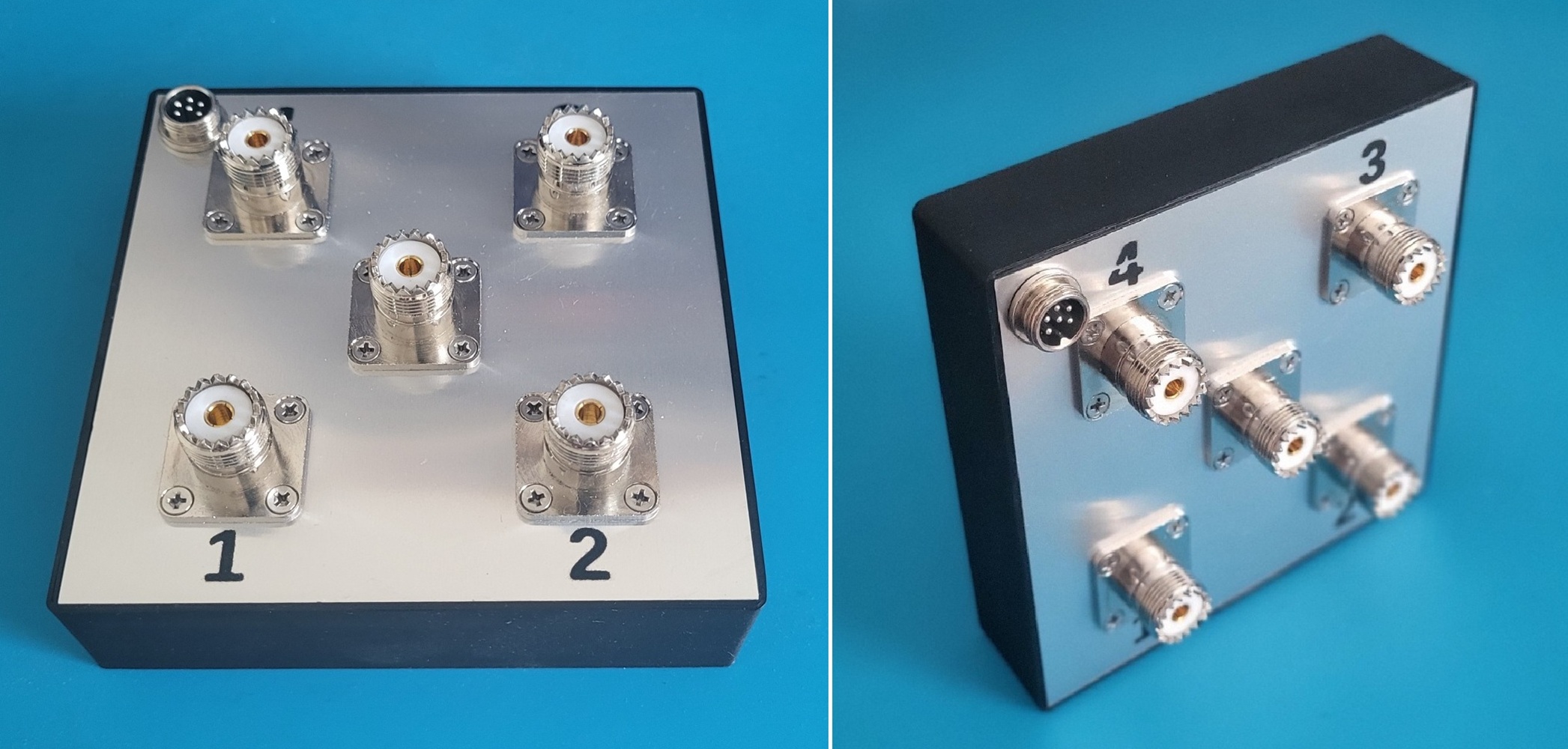
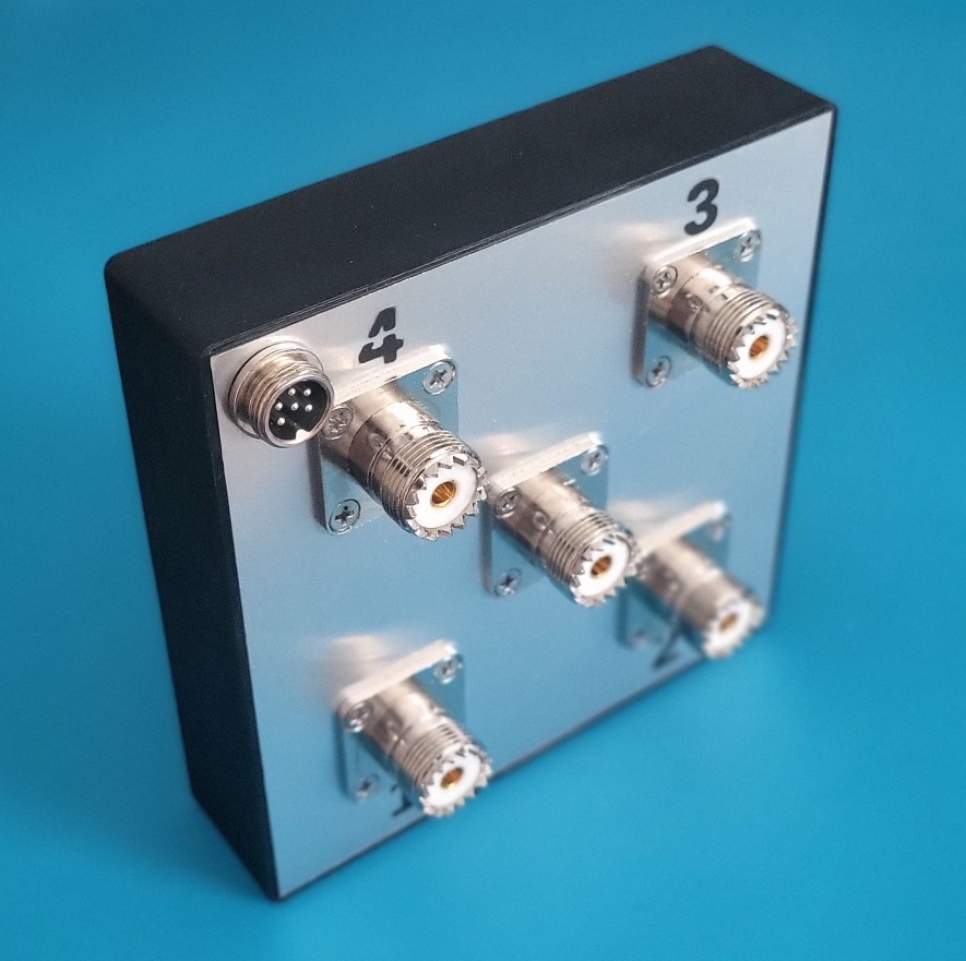
I've built two versions with identical dimensions and identical RF signal paths. The older version uses a green PCB, the newer version a blue one. The difference between the two is the option to mount the connector on the front panel, plus an added resistor divider for AS feedback, used by my Band Decoder. Both versions have identical RF parameters, and since AS feedback can be disabled in the Band Decoder's menu, either version can be used with it. If you'd like to use the feedback version (blue PCB) with your own or another commercial band decoder, that's not a problem either — just leave the feedback output pin unconnected, or simply don't populate the 4 diodes and 4 resistors on the PCB at all.
Overview
Building an antenna switch is, in theory, very simple — after all, it's just a switch with one input and two or more outputs. The trouble starts once you try to build it in practice and run into all the problems a simplified explanation conveniently ignores. With an ordinary DC (or low-frequency) switch you don't need to think about the length of the signal path, its inductance or capacitance. Often you don't even care about contact resistance or maximum power handling, because switches and relays are designed with such generous margins for everyday use. All of that changes, though, once you want to switch HF at around 1kW PEP. I already had some RF design experience, and even so, this is the fourth version — and only with this one am I finally satisfied. There's still room for small improvements, but given the cost and the uncertain outcome, I probably won't design another version.
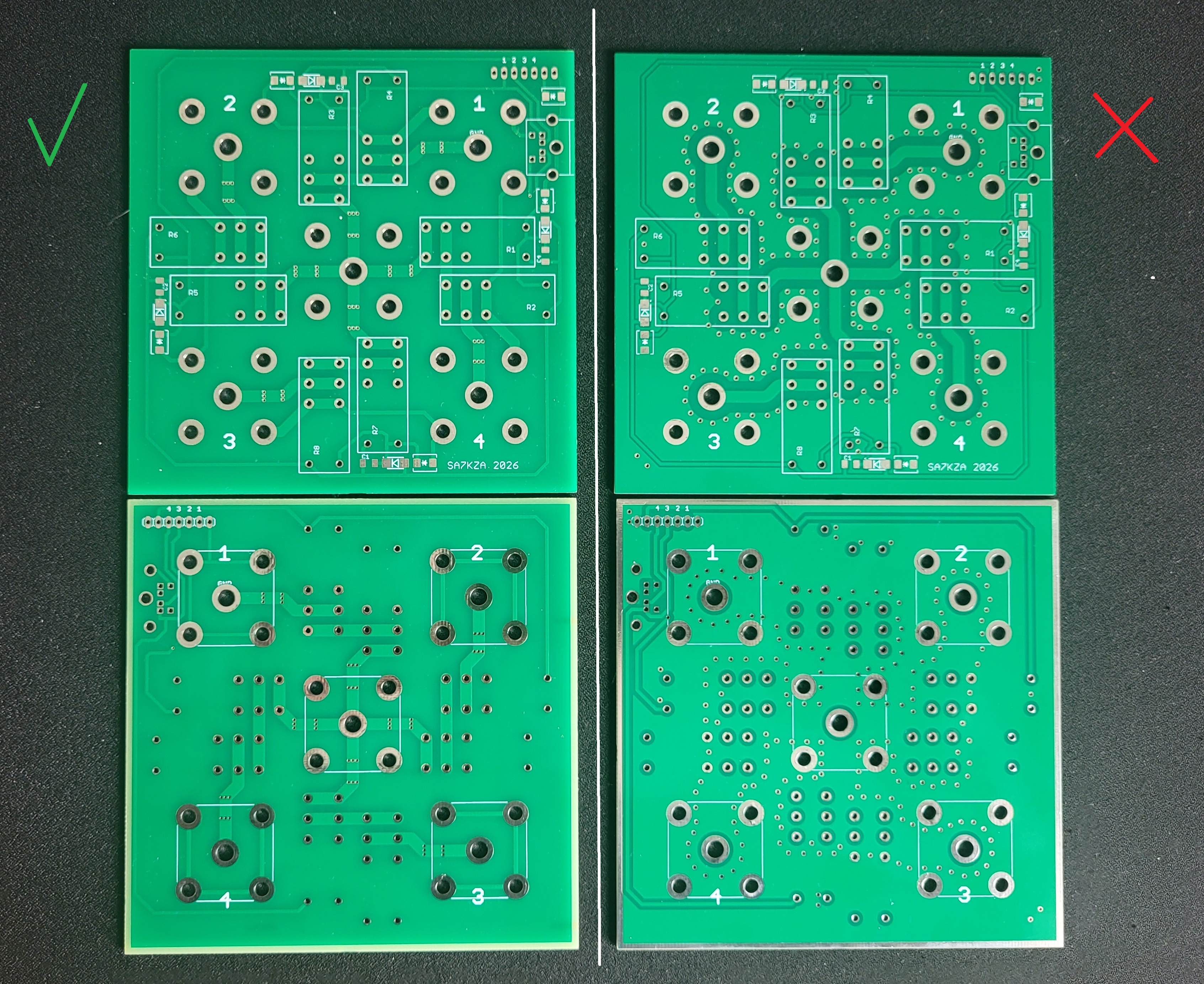
I tried a version with circular traces on the PCB, where the RF connectors' center pins were connected to the PCB with short wires. The PCB had a ground layer on both sides of the traces — coplanar ground pours flanking the trace on the same layer, plus a full ground plane on the opposite side, a configuration known as grounded coplanar waveguide (GCPW). I first tried a cheaper layout with only 4 relays, but the parameters weren't good enough for me. The 8-relay version was already decent, but according to my measurements, using a PCB with ground on both sides actually made the parameters worse. I simply don't have the budget to have 3 to 10 boards made with slightly different trace widths to hit exactly 50 ohms, and I'm sure that even if I nailed it on one batch, ordering the same board a year or two later would mean the manufacturer is using slightly different materials — and I'd be back to prototyping several variants all over again. So instead I used a method I found in old Czechoslovak Amatérske Rádio magazines: "Avoid double-sided PCBs, and keep RF traces as far away as possible from each other, and from ground." Going by my measurements, this method really does work. The photo below shows two PCBs with identical RF traces — one without ground pour around the trace, and one with it (grounded coplanar waveguide).
Circuit Diagram
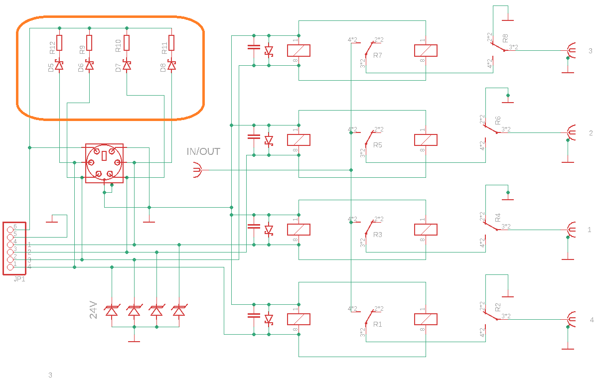
The image above shows the schematic of the antenna switch version with AS feedback. The antenna switch without AS feedback does not include the section outlined in the orange rectangle — otherwise the schematics are identical.
Worth mentioning is the approach used to achieve good port isolation and low SWR. The trick lies in the fact that relay contacts 1, 3, 5 and 7 have their second set of contacts left floating — not connected anywhere — and ideally they would not exist at all. If you were to ground them (which would effectively save you 4 relays), you would achieve a grounded centre contact on all unused antenna ports, but at the same time you would have 6 contacts (3 paired contacts) in close proximity to the active RF path. Physically, the gap between contacts is 0.5 to 1.5 mm depending on the relay type, with the width, length and spacing of the moving contact springs also playing a role. As a whole, you can think of this as 6 small-capacitance capacitors connected in parallel. For a two-antenna AS this is acceptable, and with a suitable relay choice the parasitic capacitance will not have a significant impact. This is in fact the standard way antennas are switched in transceivers and in power amplifiers up to 1 kW. The problem starts to become noticeable with three antennas, and in a four-antenna AS it is already a clearly measurable degradation. This is why in practice an additional dedicated relay is often used to ground the antenna input of each unused port. When an antenna is not in use, it is grounded by the relay at its input (for example relays 2, 4, 6 or 8), and the RF signal path between the two relays in the unused channel is left floating. The gap between the active RF path and ground is effectively doubled, since the path passes through 2 × 2 open relay contacts.
A simplified AS design using only 4 relays with unused antennas left floating achieves nearly the same SWR figures and may be worth considering. The suitability of such an AS depends on the type of antennas used. Keep in mind that particularly before a thunderstorm, some antenna types can develop voltages of hundreds of volts at the connector, and using your transceiver as a discharge path is not the wisest choice. (This of course does not apply to all antennas, and depends not only on the antenna itself but also on its feed point.)
AS feedback and how it works is described in the Band Decoder project. The remaining components are protective: a standard blocking diode at each relay, and a small-value capacitor for RF filtering. Each control input also has a protective bidirectional ESD protection diode, though this isn't really necessary for a short indoor cable installation — it becomes useful only when the AS is mounted at the end of a long cable, close to the antennas.
PCB
If you look at the board you may notice — most visibly around the centre/common connector — that not all mounting pads are connected to ground. This is intentional. Bear in mind that the ground connection is achieved through the top aluminium panel, to which each of the five connectors is attached via four M3 screws. The aluminium is 1.6 mm thick with a copper layer on the underside, so the mutual bonding between connectors can hardly be improved upon, and a dedicated ground path on the PCB itself is simply not needed for the RF signal. Ground traces on the PCB are provided only for the control logic and protection components.
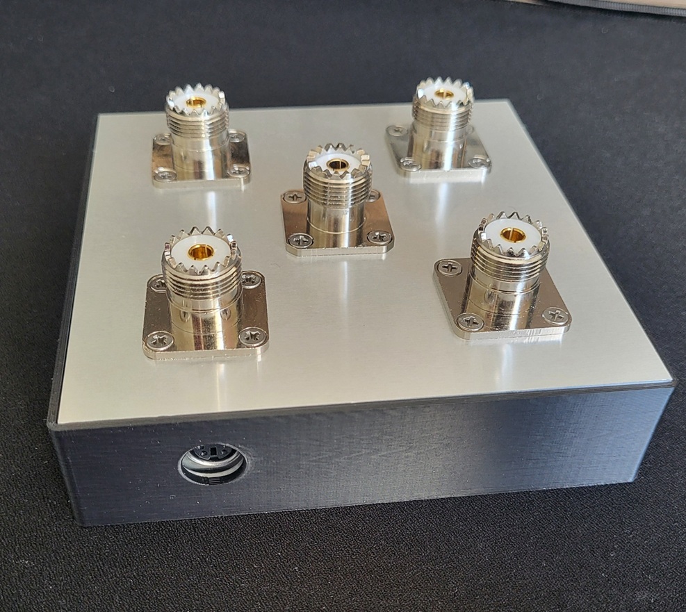
The connection between the BD and the AS can be made in several ways. One is via a connector with pins on the side of the AS (the same connector used in the Band Decoder and the Interface for the Yaesu rotator projects). The blue PCB version also allows a 6-pin connector on the front panel, which in some cases simplifies mounting the AS into an enclosure. The last option is to skip the connector altogether and solder the cable directly to the PCB.
Connector Panel Assembly
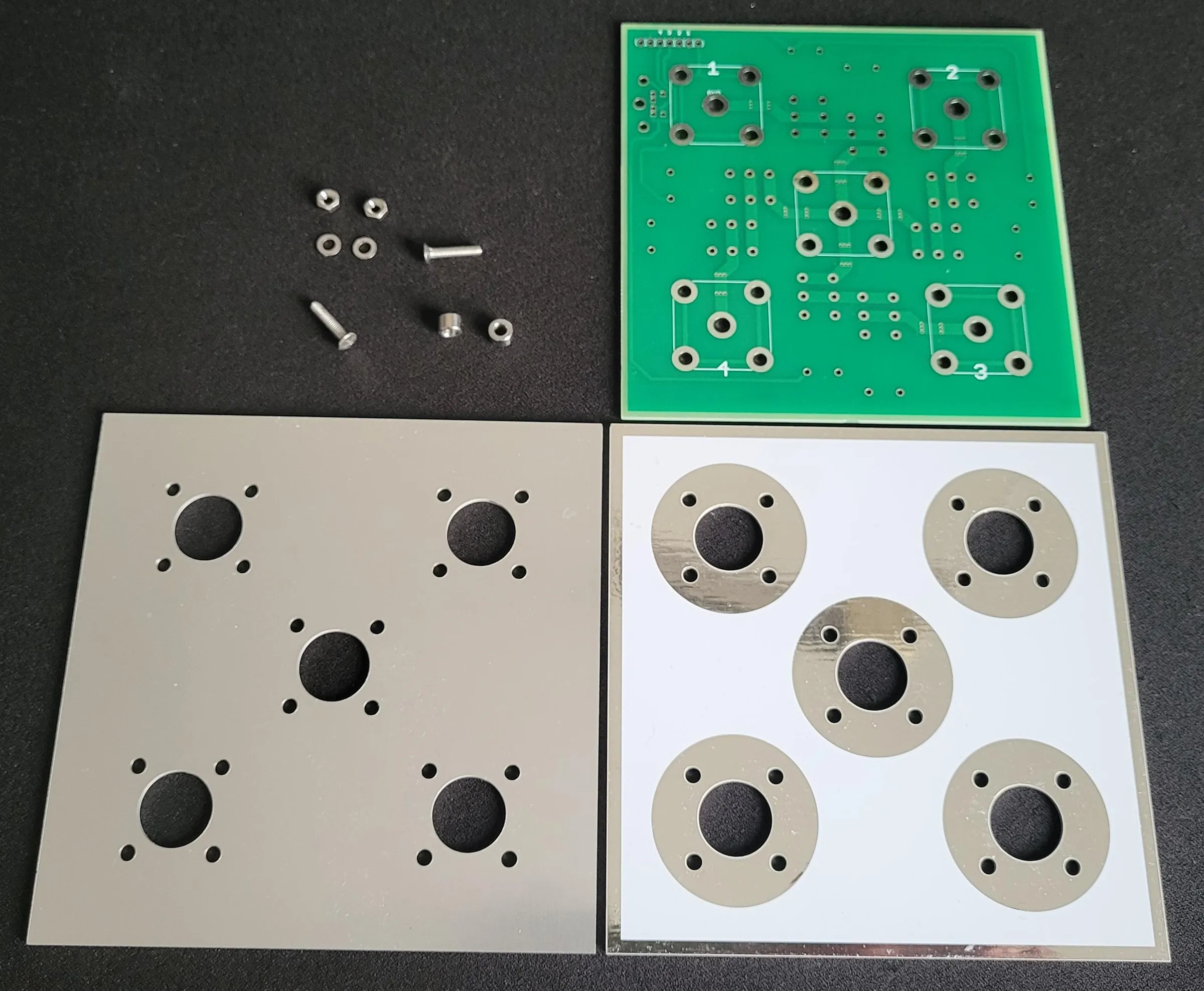
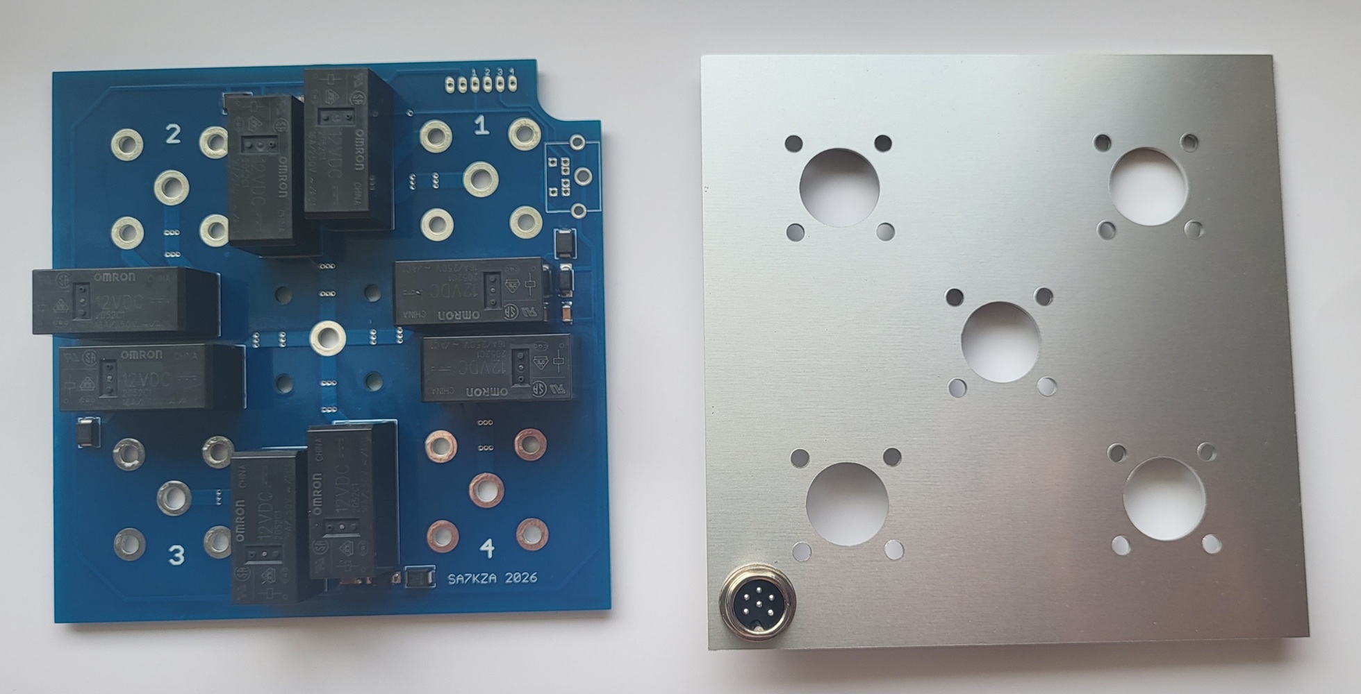
As mentioned earlier, the top panel (connector panel) is made from aluminium PCB. On one side of this board is a 1.6 mm aluminium sheet, on the other side is a copper layer, with a dielectric layer between them. These PCBs are typically used where heat dissipation is required — for example in LED panels. For our top panel the dielectric layer is an unwanted complication, however when you consider that each connector has 4 mounting holes through which metal screws pass — connecting the copper and aluminium layers at a total of 20 points, right in the area of the connectors — the two layers can be considered very well bonded, and this holds true across the entire HF spectrum. You can of course use a plain aluminium sheet instead. I chose aluminium PCB primarily for cost and hole accuracy. Anyone who has tried drilling clean, precise 16 mm holes in aluminium knows it is not as straightforward as it sounds — and then there are another 20 holes of 3.2 mm diameter to deal with.
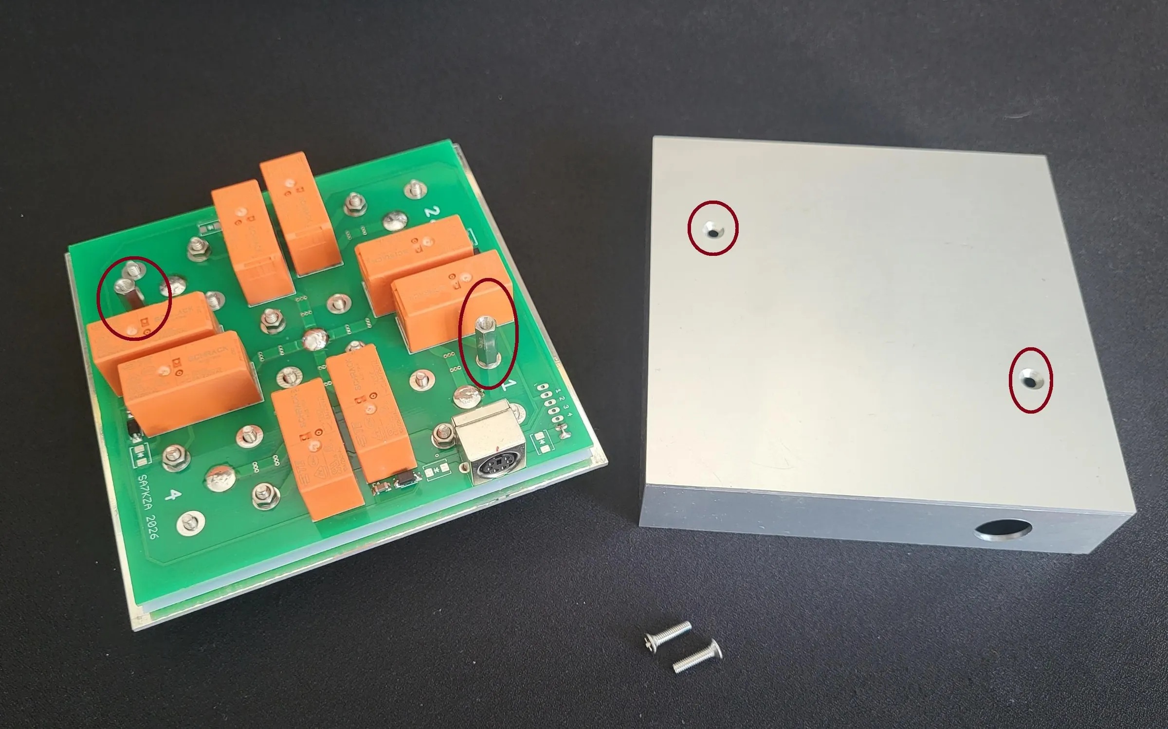
In the image you can see the connector panel from both sides. In the area of each connector the copper layer is exposed and tinned. Also note that the green PCB carrying the relays is slightly narrower — this is because the side walls of the enclosure will also be made from aluminium PCB, requiring at least 1.6 mm to be added on each side. I chose to add a little more so that the connector panel also overlaps part of the 3D printed outer plastic shell of the AS.
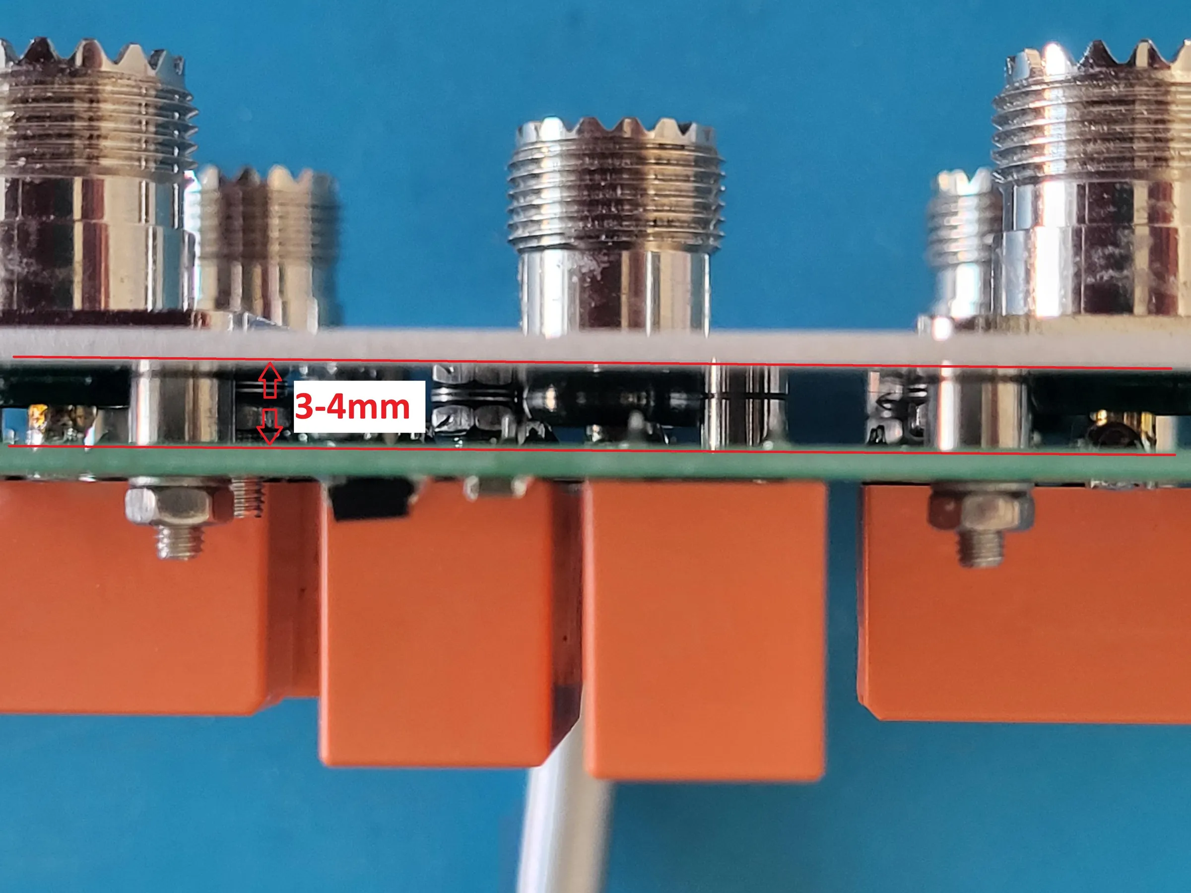
Also visible in the image are the metal standoff spacers, 3–4 mm tall, which create a gap between the top panel and the green PCB. 3 mm standoffs are easier to source and will work fine. I used 4 mm standoffs simply because I had them on hand. It is not necessary to use a standoff at every joint — 6 or 10 standoffs is sufficient, with a nut and washer placed on the tinned copper surface at the remaining positions. It is important that standoffs are used at the joints that will later be used to connect the top and bottom parts of the aluminium enclosure — at these positions a 12–14 mm threaded standoff will be used on the green PCB side instead of a nut. (A nut can be used temporarily on the green PCB side during assembly.)
You will find that joining the connector panel to the green PCB is not entirely straightforward — there are 20 holes with 20 screws to manage. It requires a bit of patience and dexterity. I found it helpful to use adhesive tape on the connector side to hold the screws in place so they wouldn't fall out. I then worked them through the holes in the PCB one by one, fitted a washer and secured each with a nut. In the second image you can see the gap between the connector panel and the green PCB.
Now centre the two boards relative to each other and tighten all the nuts. The connector pins are already inserted into the PCB and even though they are not yet soldered, contact is made — and you can already measure the SWR. It should be below 1:1.1, most likely below 1:1.05. (Remember to calibrate your VNA before measuring, using the actual cables and load you intend to use.)
If the SWR is within spec, you can now solder the connector pins. From this point you have a functional AS — all that remains is to build the enclosure, ideally also from aluminium to provide proper RF shielding. Let's get to it...
Completing the Aluminium (inner) Enclosure
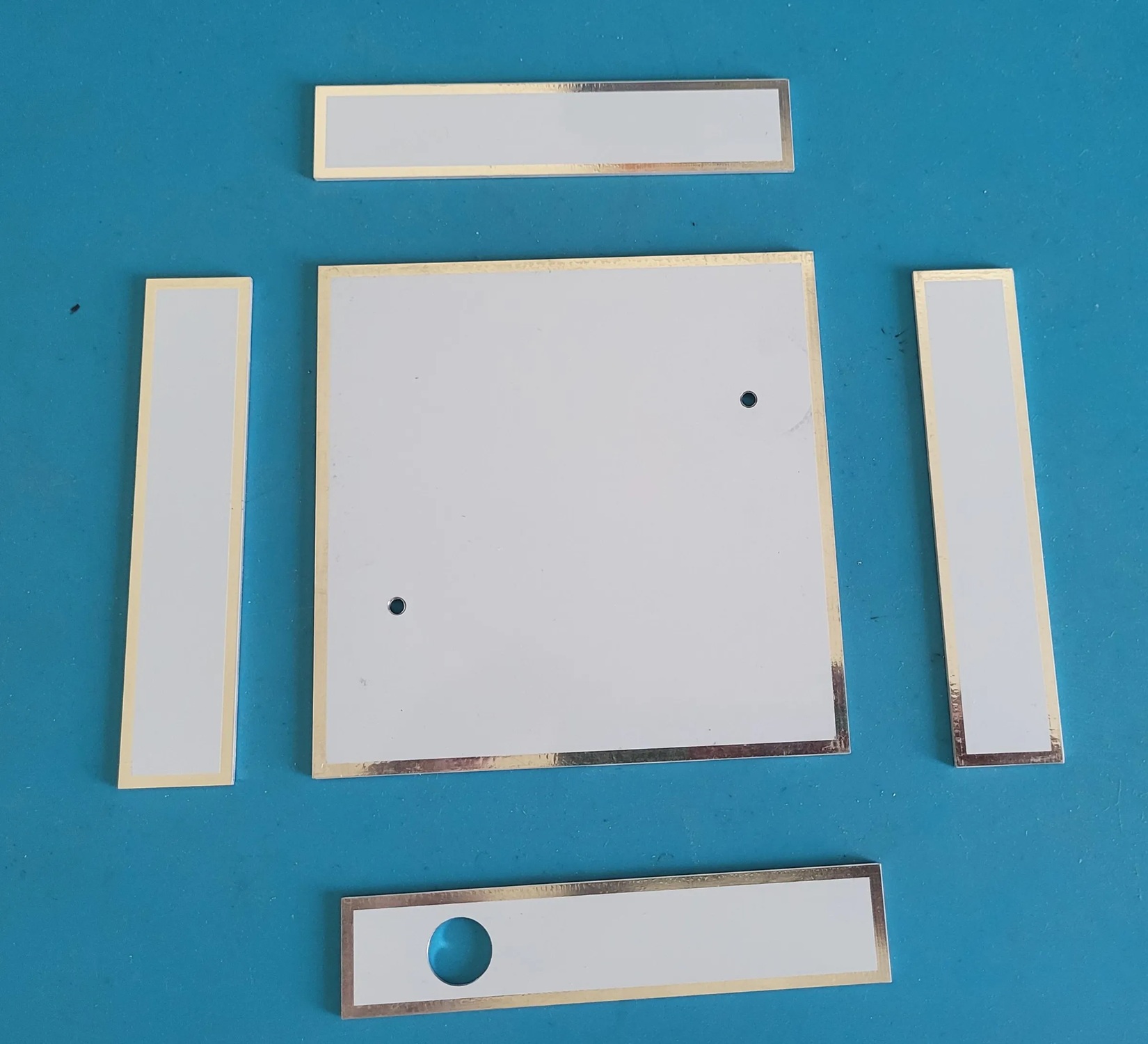
This is technically the most demanding part of the build. The individual parts can be seen in the first image. Prepare everything first before joining any pieces together.
All parts are made from aluminium PCB. The exact outcome will depend on what you ordered from your manufacturer. The minimum order quantity at my supplier is 5 pieces. Since there are 4 side walls, I can use almost all of them with one spare. As I did not plan to build more than one AS, I ordered only the minimum quantity the first time around. This means I had to manually drill the opening for the PS/2 6-pin connector in one of the side walls. The position of this hole depends on the height of the standoff spacers and the dimensions of the side walls — this is individual to your build, so you will need to measure and calculate the position yourself. The hole diameter is 13 mm. As already mentioned, drilling a clean and accurate 13 mm hole in aluminium is not entirely straightforward. I used a bench drill press and a carbide hole saw.
I then drilled two 3.2 mm holes in the rear panel for the screws that join the connector panel to the rest of the enclosure. Their position must match the position of two of the connector mounting holes — as discussed earlier. You can choose any connector holes you like, but they must be the ones fitted with standoff spacers so the PCB does not flex when tightening. It is convenient to plan for these holes already when designing the enclosure PCB. Finally, these two holes are countersunk on the aluminium side to accept flat-head screws. At this point everything is ready.
Now we join the individual parts together. We will use the exposed copper layer along the edges of the panels, which we had pre-tinned during production. I should warn you that this will not be easy — you need to balance precision, speed, the thermal conductivity of aluminium, and the power of your soldering equipment. I do own a 250W soldering iron which I use occasionally, but it is large and heavy. For this job I chose to use a heated plate, which costs around €50 and is excellent for desoldering PCBs — and with a little skill also for soldering SMD components (but that is a topic for a separate article).
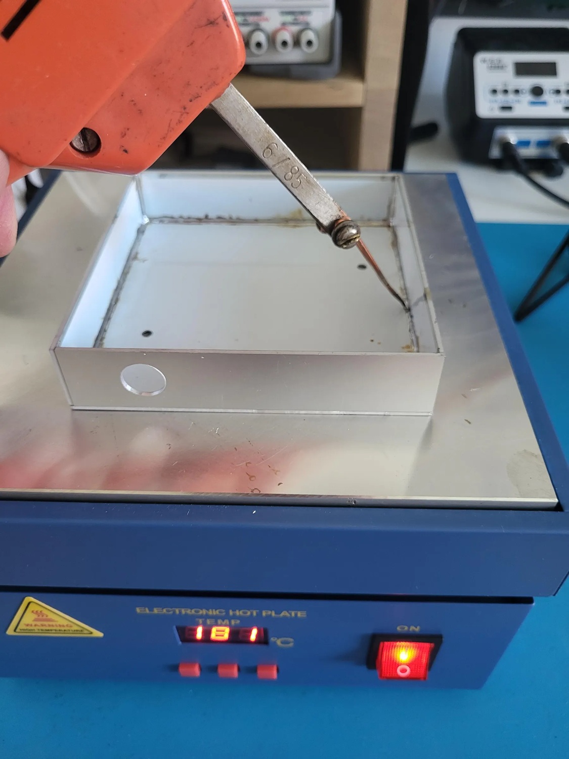
I first allowed the plate together with the parts to heat up to 180°C, then used a transformer-type soldering gun to solder the remaining parts together. It sounds straightforward but it took at least half an hour before I was satisfied with the result. Finally I cleaned up the excess flux residue and the result is visible in the image.
Outer Enclosure
The soldered aluminium enclosure, while fully functional and sufficiently rigid, requires some surface finishing. If we are going to build something, it might as well look good too. I decided to place the enclosure inside an additional outer shell. Nowadays it is easy and affordable to design and 3D print almost anything, with very good results. I use ASA material almost exclusively — it is durable and sufficiently UV resistant, and has proven itself well even in outdoor applications. The outer shell consists of two parts: a bottom and a lid. The 3D model can be downloaded from the attached files. The AS slides into the bottom part up to its edge. You can leave it like this as it already looks good, or add the top lid with channel numbers. I haven't decided yet which I prefer 🙂. The bottom and lid can be bonded together using acetone, creating a permanent enclosure. Permanent enclosures are now standard practice, and there is really nothing to repair inside an AS anyway — either it works or it doesn't. Relay replacement is possible, but it is a genuinely demanding operation that requires proper equipment.
