(HW3) Automatic HF Band Decoder for ICOM & Kenwood
The control unit for an automatic antenna switch — selecting the right antenna automatically based on the band you're on, for Icom and Kenwood HF transceivers.
Introduction
This project grew out of the need to switch antennas automatically — something that makes life much easier during local operation, but becomes almost essential for remote station control, which keeps growing in popularity. This is the third generation of the Band Decoder (BD for short), hence the HW3 designation.
The first version could drive 12 antennas (one per band) using GND-switched logic. It later turned out that commercial antenna switches (AS) mostly use VCC-switched logic instead, so the next version (HW2), which I published on Instructables, moved to a UDN2987 driver array — which, as a bonus, protects the outputs against short circuits, so a shorted cable to the antenna switch or a clumsy installation mistake won't damage the BD. This third version builds on practical experience running HW2, where it became clear that 12 channels were simply more than anyone would ever use. Since the connector between the BD and the AS has stayed the same since HW1, switching the logic from GND to VCC left one pin on that connector unused. This new version puts that spare pin to work: it monitors which relay is actually receiving voltage, so the BD can now detect whether the correct relay is being switched — or catch a fault in the interconnecting cable.
Key Features:
- Detects all HF bands plus 6m and 11m
- 8 independent channels (4 with relay feedback monitoring)
- 1.8" TFT LCD display
- Fault detection
- Built-in menu system — all settings adjustable on-device, no reprogramming required
If you have at least some experience with the Arduino UNO and the Arduino IDE, you can use this project as a base to build your own Band Decoder.
Overview
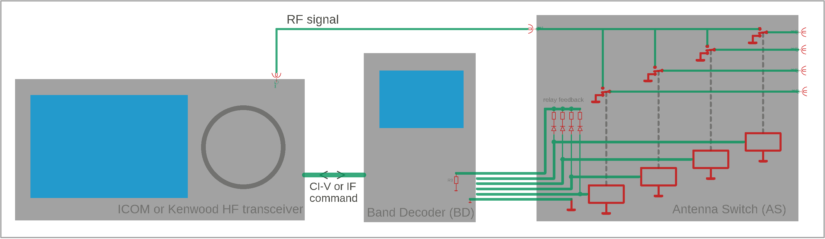
The Band Decoder connects to the transceiver through a communication interface. On Icom radios this is a 3.5mm jack carrying CI-V, and the BD has a matching 3.5mm jack on its side. Kenwood radios instead communicate with the Band Decoder over a COM port; the device is designed for a straight RS-232 cable (a null-modem / crossed cable will not work).
The working principle is straightforward. At regular intervals the Band Decoder asks the transceiver: "What frequency are you on right now, and are you in TX or RX?" The transceiver replies, for example, "I'm currently on 14.200 MHz, in RX mode." The BD's firmware processes that reply and notices that the band has changed since the last update — say, from 10m to 20m. Since the transceiver is in RX mode, making the switch safe (hot-switching a relay while transmitting could damage its contacts, or even the transceiver's PA), it turns off the 10m output and turns on the 20m output. In the electronic antenna switch, the 10m relay releases, dropping back to its resting, grounded state, while at the same moment the 20m relay — which had been resting in its grounded state until now — activates, breaking that ground connection and connecting the transceiver's RF input/output to the 20m antenna instead.
Inside the antenna switch, each relay's own resistor connects to the shared relay-feedback line through a diode — so current can only flow one way, and no single branch can feed voltage back into another relay's resistor. Together with resistor R9 back in the Band Decoder, each relay's resistor forms a voltage divider on that shared line, so every active relay produces its own distinct voltage. The BD measures this voltage and compares it against the value stored during configuration. If the voltage doesn't match, an error is shown on the display. Since not every commercial antenna switch supports relay feedback, this check can simply be disabled in the menu for those that don't.
Circuit Diagram
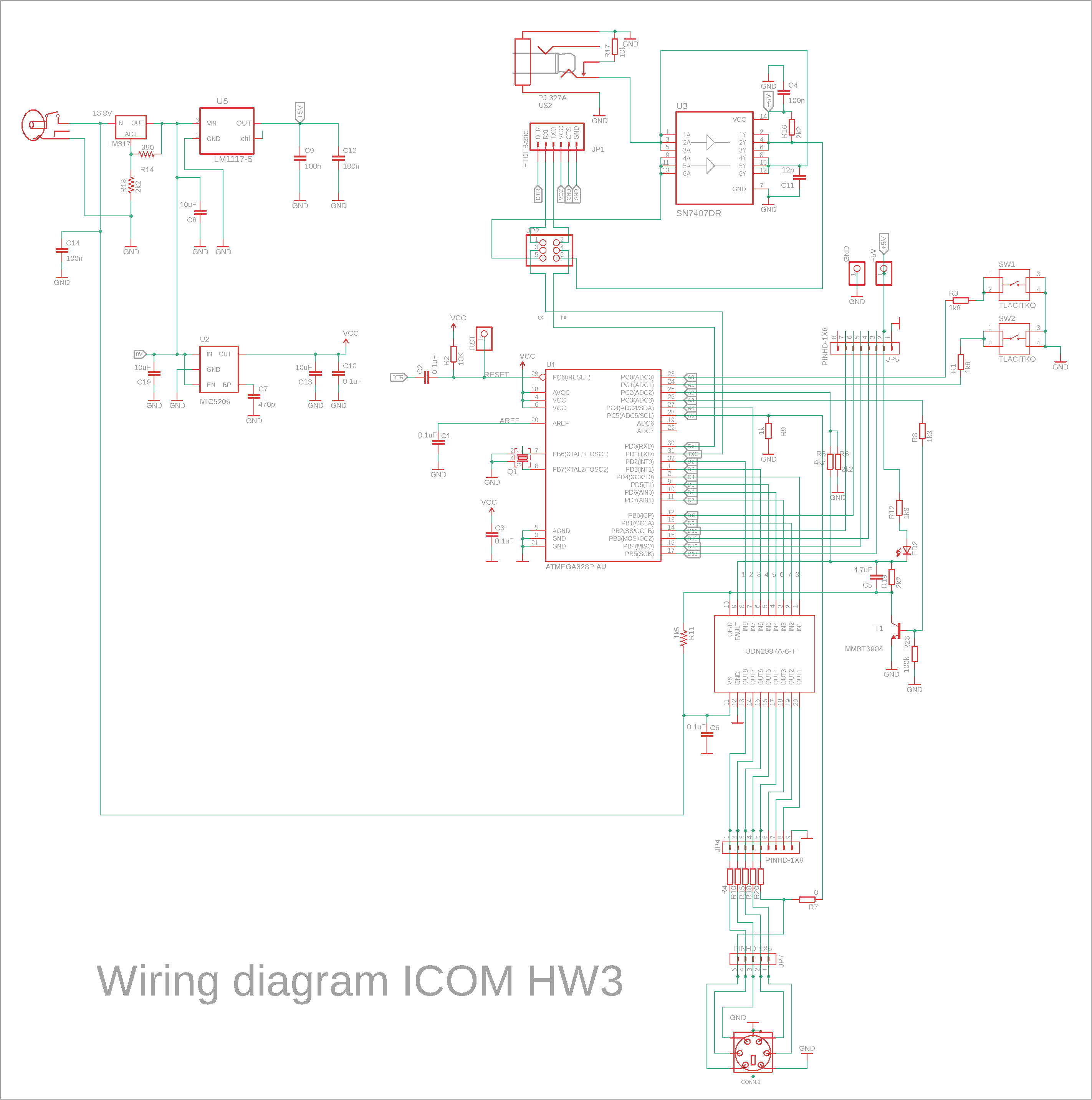
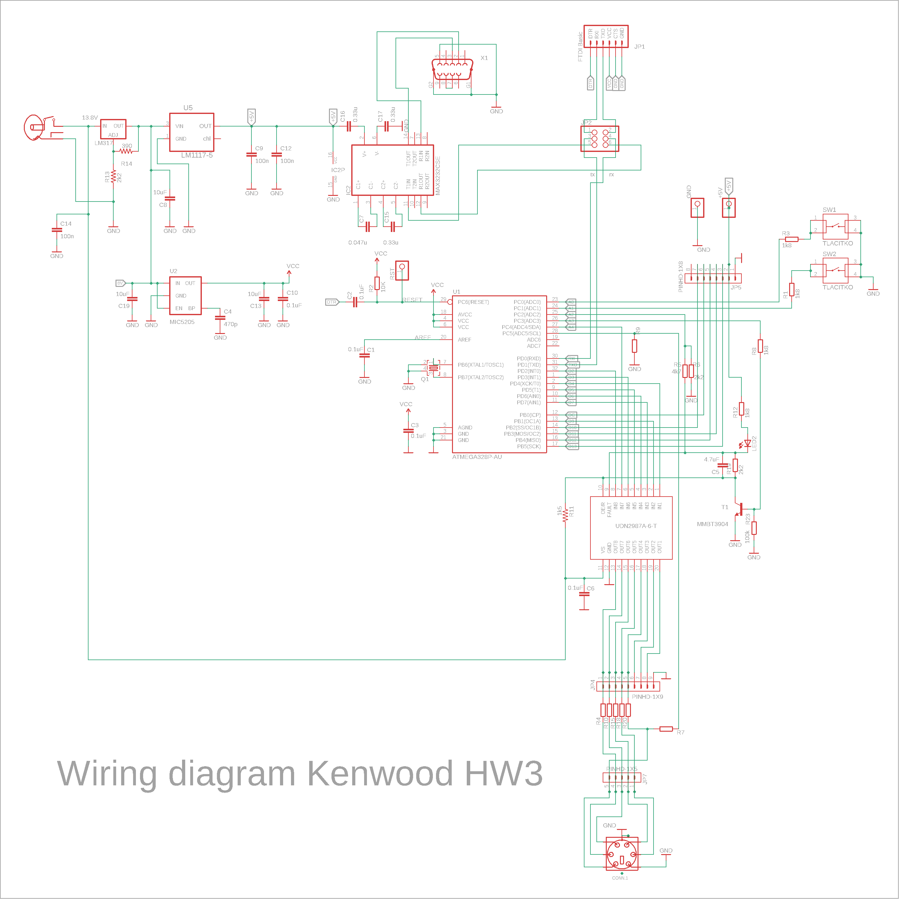
As you can see, the Icom and Kenwood schematics are very similar — aside from the input stage, they're identical.
The Icom version uses an SN7407 on its input, wired to split the single-wire CI-V signal into separate RX and TX lines feeding the ATmega328P-AU MCU (yes, the same MCU used on the Arduino UNO — which comes in handy later when programming it).
The Kenwood version instead uses a MAX3232 RS-232 level converter on its input, which brings the RX/TX signal to the correct levels for the MCU. It's important to stick to the component values shown around the converter, or you may run into signal issues. Connector pins 7 and 8 must be bridged together.
Everything described from here on applies equally to both BD variants.
Jumpers on the PCB let you switch the MCU's TX/RX lines between "W" (Work) and "P" (Programming). In the P position, the MCU's RX/TX pins are connected to the programming header; in W, they're connected to the SN7407 or MAX3232 converter instead.
The control buttons are wired to the MCU's A0 and A1 pins. The A5 analog input reads the voltage from the relay-feedback divider described above. A2 picks up the FAULT signal from the UDN2987A after it's been level-shifted. Output A3 drives transistor T1, which resets the UDN2987A whenever a fault is detected.
The display is wired up in the standard way and connects via connector JP5 (the display itself isn't shown on the schematic).
The remaining 8 I/O pins connect to the UDN2987A driver array, since the MCU's own outputs aren't strong enough to drive the relays directly.
The UDN2987A is officially marked as not recommended for new designs, but it has one feature that made me pick it anyway: built-in overload protection. Short its output, and the chip won't blow — it just shuts that one output down. That's a genuinely useful trait, and newer replacement chips have dropped it; reproducing the same behaviour with discrete parts would take a lot more components. Unfortunately, the chip's well-known weak point is switching inductive loads, and the manufacturer never fully solved that. I found that adding C5 and R19 almost eliminates the problem, but I added fault monitoring and control on top, just to be safe.
The power supply section is maybe a bit more elaborate than it needs to be, but it's a design that's worked well for me. Since we're measuring voltages, the MCU needs a clean, accurate supply — that's what the MIC5205 is for. The rest of the BD runs off a simple, cheap LM1117-5. Both regulators are fed from an LM317, which takes the usual 13.8V hamshack supply on its input and drops it to roughly 8V on its output, spreading the heat dissipation more evenly across two stages. A switching regulator could obviously replace the LM317 here, but this is a proven design I reuse across several projects.
Resistors R7 and R20 decide what the sixth pin of the output connector is used for. Fit R7 = 0Ω and leave R20 unpopulated to use relay feedback; fit R20 = 0Ω and leave R7 unpopulated instead, and that same pin lets you drive a 5-channel antenna switch from the output connector.
PCB
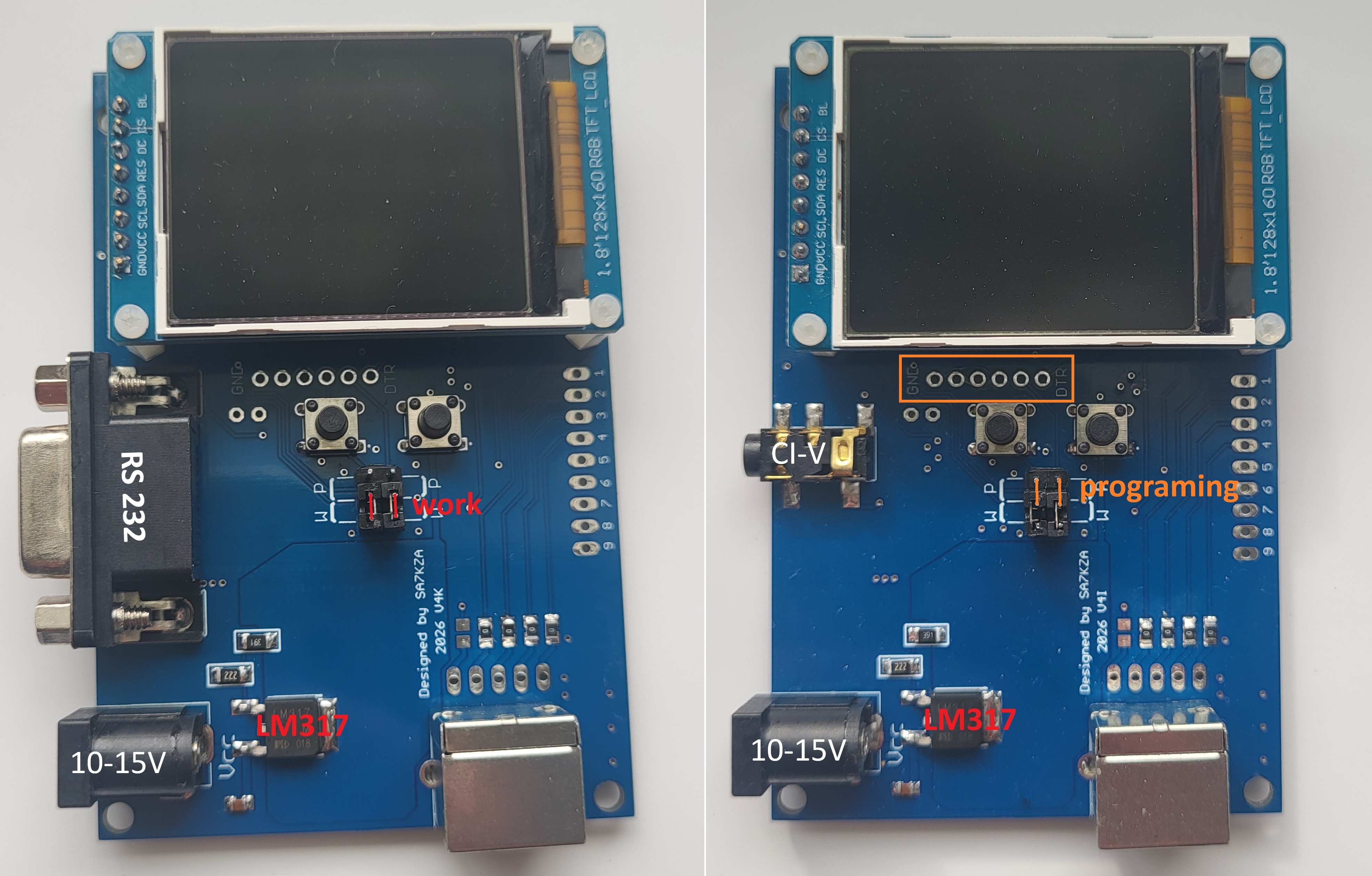
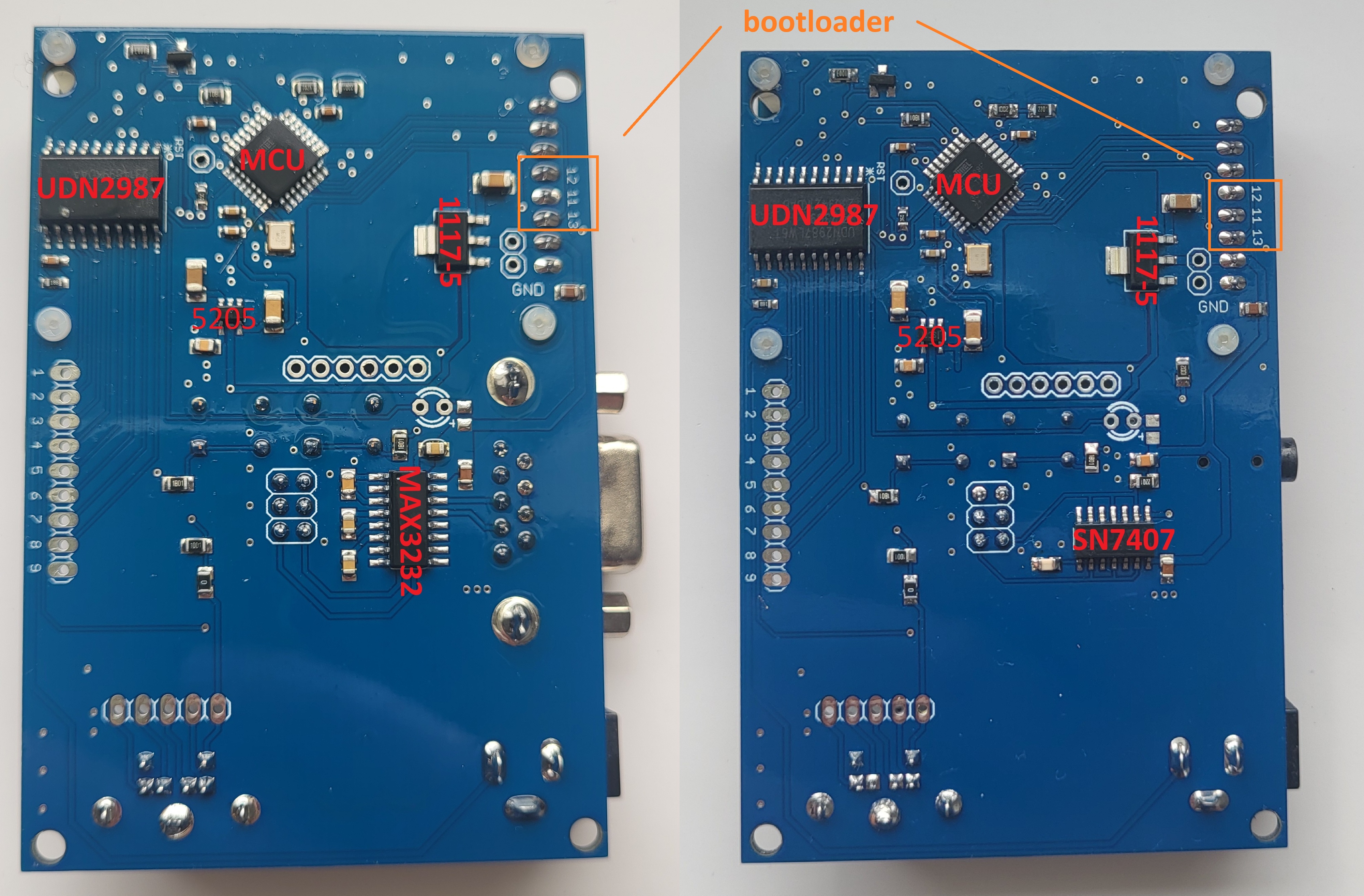
These photos show the assembled double-sided PCBs for both the Icom and Kenwood versions. They're the same size, and at a glance you can tell them apart by the input connector: the Kenwood board, on the right, has a fairly large 9-pin RS-232 connector, while the Icom board, on the left, has a small 3.5mm jack connector — the kind you'll probably recognize from audio headphones.
Marked in orange under the display is the connector for a USB-to-TTL serial adapter (often called an FTDI adapter/programmer). This connector is used to upload firmware to the MCU. In the second photo, pins 11, 12 and 13 are highlighted — these are used for burning the bootloader. We'll go into that in more detail in the next section.
Start by soldering all the components on the MCU side. Alternatively, you can have the PCB assembled with that one side already populated — that's what I usually do myself. The downside is you'll need to order at least 5 boards.
Then, following the procedure below, burn the bootloader into the MCU, and only after that populate the other side of the PCB.
Of course, you can also populate the entire PCB in one go, but that makes burning the bootloader a bit trickier.
Firmware
As you probably know, every MCU runs according to a program — an algorithm called firmware — which can be written in a number of programming languages. I got into programming fairly late myself, and like many others, I started with Arduino and the Arduino IDE. It's well documented and beginner-friendly. To make programming easier, the MCU uses a small helper program called a bootloader:
"Microcontrollers are usually programmed through a programmer unless you have a piece of firmware in your microcontroller that allows installing new firmware without the need of an external programmer. This is called a bootloader."
We're essentially building our own version of an Arduino Uno here, but the board doesn't need a permanent USB port for normal operation. Why add extra components, more complexity, and a bigger PCB for something you'd only ever use once? Instead, we just plug a USB-to-TTL adapter into the connector — without soldering it in — only when we need to upload firmware to the MCU.
The bootloader is what lets a PC running the Arduino IDE talk to the MCU over its RX/TX pins.
There's also another way to get firmware onto the MCU — for example using a dedicated programmer such as the SparkFun Tiny AVR Programmer (often just called a "Tiny AVR ISP"), which uses the MCU's dedicated programming pins directly. That would work fine in our circuit too, since those pins are already wired to the display in the standard way and the layout needs no changes for it. That said, we'll stick with the bootloader approach — admittedly more out of habit and history than necessity — so the board behaves just like an Arduino Uno.
What you need
- Arduino UNO used as a programmer. The Arduino UNO can act as an ISP (In-System Programmer).
- USB cable for the Arduino UNO
- Target board with an ATmega328P (our Band Decoder board)
- A few jumper wires
Programming method
- Connect the Arduino UNO to your PC.
- Open the Arduino IDE.
- Open File → Examples → ArduinoISP.
- Upload this sketch to the Arduino UNO.
- Wire the Arduino UNO to the target microcontroller using the ISP signals: 11→11, 12→12, 13→13, 10→RST, VCC→VCC (use the VCC pin on the programmer connector), GND→GND.
- In Tools → Board, select "Arduino Uno".
- Click "Burn Bootloader".
After this step, the microcontroller behaves like a standard Arduino Uno and can be programmed normally via the serial interface.
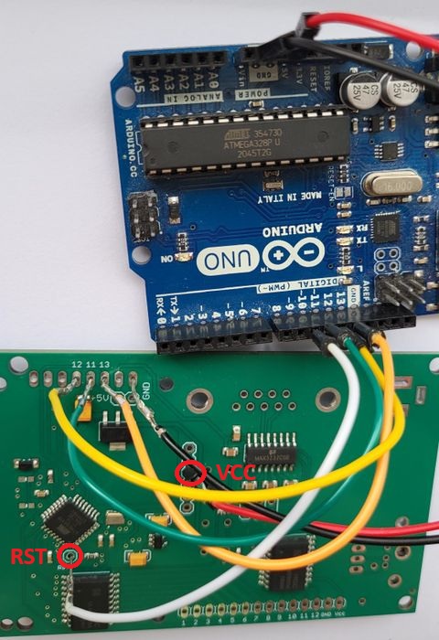
Before uploading any code, make sure all components are populated on the PCB. The BD doesn't need to be connected to its power supply for this — VCC reaches the MCU through the programmer's own VCC pin.
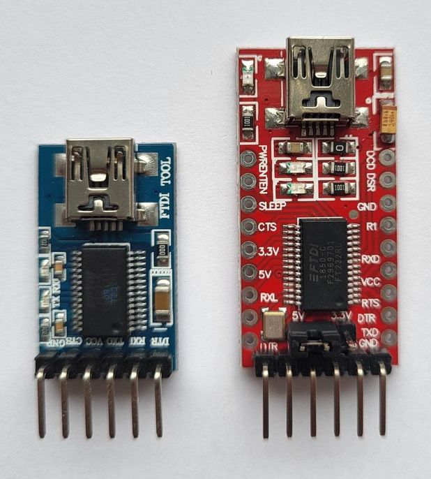
To upload the actual firmware, you'll need the USB-to-TTL adapter mentioned earlier. The photo below shows the two adapter versions I use myself — it doesn't matter which one you use, what matters is the pin order on the connector. The PCB is designed for the pin order DTR – RX – TX – VCC – CTS – GND. If your adapter has a different pin order, just use jumper wires — the same kind you'd find in beginner electronics kits — to match it up.
Before uploading any code, move both jumpers to the "P" (Programming) position, as shown in the PCB photos earlier.
Insert the programmer's pins into the holes, hold it gently in place by hand, and tilt it down to roughly an 80° angle — however far the pins and holes will let you go. This creates a temporary connection that's perfectly good enough for programming. With the programmer held in place like this, upload the code to the Band Decoder (which now behaves like an Arduino Uno board) exactly the way you'd normally program an Arduino Uno.
Once the upload finishes successfully, remove the programmer and don't forget to move both jumpers back to the "W" (Work) position.
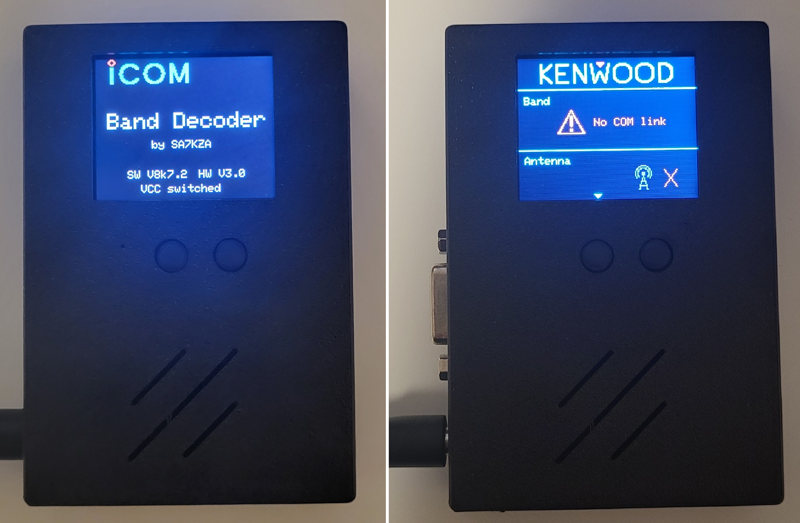
Connect the power supply and the BD will start up. After the splash screen, it will show the Icom or Kenwood logo, and since there's no transceiver connected yet, the display will show a "No COM link" error. At that point, you know the BD is working correctly and the MCU is doing its job.
Enclosure
The 3D model of the enclosure was designed in OpenSCAD and printed on a 3D printer using ASA. It's made of two parts that snap together and are held with two screws. Below you can see both the Icom and Kenwood versions — the .stl files can be downloaded in the Download section.
Notes
This page isn't a complete build guide. It should still make building your own version significantly easier, though, since you can reuse the same operating principle and a hardware design that's already proven itself.
The basic communication firmware — without EEPROM storage, the menu system, or the protection features — isn't complicated at all (a few hundred lines). The finished firmware, though, runs to more than 3700 lines, and I'd rather it didn't just spread around the internet uncontrolled. So for now it's available on request only, on the condition that it isn't redistributed or modified further.
As Icom uses the same "protocol" for all radios with a CI-V 3.5mm jack, the device should work on all such Icoms. Tested on the 7300 and the much older 706. Here is the list of compatible rigs: IC-7300MK2, IC-7760, IC-7610, IC-7300, IC-7100, IC-9100, IC-7410, IC-7600, IC-7700, IC-7200, IC-7000, IC-703, IC-7800, IC-756 Pro III, IC-756 Pro II, IC-746 Pro, IC-756 Pro, IC-718, IC-746, IC-706 MkIIG, IC-756, IC-706 MkII, IC-706.

